[vc_row][vc_column][vc_column_text]
[/vc_column_text][vc_empty_space][/vc_column][/vc_row][vc_row][vc_column][vc_custom_heading text=”Key Benefits” google_fonts=”font_family:Actor:regular|font_style:400 regular:400:normal”][vc_empty_space height=”15px”][vc_column_text]
PROCESS FLEXIBILITY
The RF match box wide operating range (from 100 W to 2000 W) accommodates a wide range of customer applications in RIE, ICP-RIE, and ICP-CVD modes
The vacuum load lock enables using a combination of fluorinated and chlorinated chemistries in the same tool
BEST REPRODUCIBILITY
Load lock operation and heated chamber walls offer stable and repeatable process conditions
Novel cathode design and efficient helium back side cooling of the shuttle and substrate ensure uniform temperature control during deposition
BEST REPRODUCIBILITY
Load lock operation and heated chamber walls offer stable and repeatable process conditions
Novel cathode design and efficient helium back side cooling of the shuttle and substrate ensure uniform temperature control during deposition
HIGH UPTIME
The reactor’s heated walls enhance plasma cleaning efficiency and reduce cleaning requirements
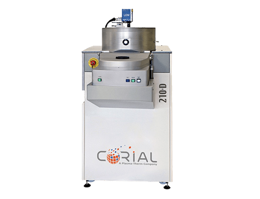
Only 15 minutes are required to perform a reactor clean[/vc_column_text][vc_empty_space][/vc_column][/vc_row][vc_row][vc_column][vc_custom_heading text=”Related processes” google_fonts=”font_family:Actor:regular|font_style:400 regular:400:normal”][vc_empty_space height=”15px”][vc_column_text]The Corial 210D can serve a variety of applications in specialty semiconductors markets including:
- Advanced Packaging
- Wireless Communication
- R&D
[/vc_column_text][vc_row_inner][vc_column_inner width=”1/3″][vc_column_text]
Low temperature Silicon Dioxide (SiO2) ICPCVD deposition process
[/vc_column_text][vc_empty_space height=”10px”][vc_single_image image=”14569″][vc_empty_space height=”10px”][vc_column_text]R&D
- Deposition rate 140 nm/min
- Refractive index 1.47
- BOE etch rate < 110 nm/min
[/vc_column_text][/vc_column_inner][vc_column_inner width=”1/3″][vc_column_text]
Fast Silicon Nitride (Si3N4) ICPCVD deposition process
[/vc_column_text][vc_empty_space height=”10px”][vc_single_image image=”14570″][vc_empty_space height=”10px”][vc_column_text]Advanced packaging
- Deposition rate 150 nm/min
- Deposition temperature 70°C
- Stress -100 ± 50 MPa
[/vc_column_text][/vc_column_inner][vc_column_inner width=”1/3″][vc_column_text]
Fluorinated Silicon Oxide (SiOF) ICPCVD deposition for SAW devices passivation
[/vc_column_text][vc_empty_space height=”10px”][vc_single_image image=”14571″][vc_empty_space height=”10px”][vc_column_text]Wireless Communication
- Deposition rate 170 nm/min
- Deposition temperature 70°C
- Refractive index 1.42
[/vc_column_text][/vc_column_inner][/vc_row_inner][/vc_column][/vc_row]
